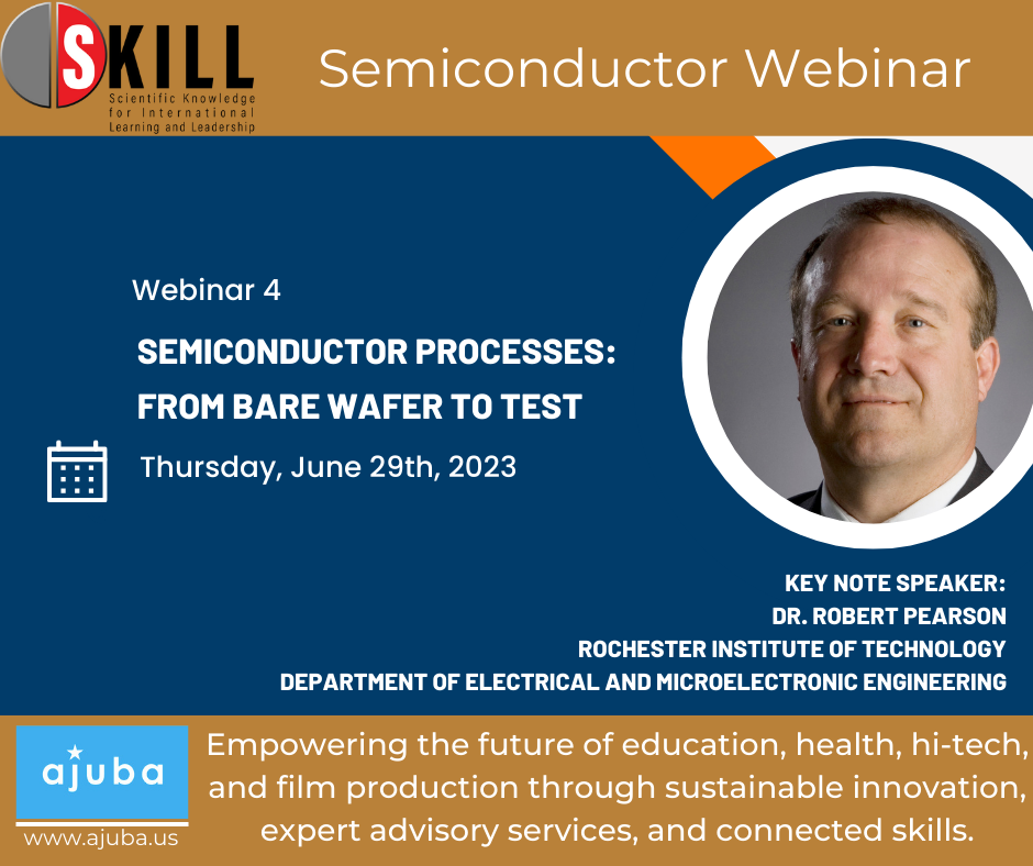
Watch the insightful webinar on semiconductor processes that was held on June 29th, 2023. In this video you will explore the journey of a semiconductor device from its bare wafer stage to the final testing phase. This webinar will provide a comprehensive understanding of the various steps involved in the fabrication and testing of semiconductor devices.
Key Topics to be Covered:
1. Introduction to Semiconductor Processes
- Overview of the semiconductor industry
- Importance of semiconductor processes
2. Wafer Preparation
- Wafer cleaning and surface preparation techniques
- Introduction to photolithography and mask preparation
3. Semiconductor Fabrication Techniques
- Deposition processes (CVD, PVD, ALD)
- Etching techniques (wet etching, dry etching)
- Ion implantation and doping processes
4. Backend Processes
- Backend wafer processing (backend-of-line, front-end-of-line)
- Interconnect fabrication and packaging techniques
5. Testing and Quality Control
- Importance of testing in semiconductor manufacturing
- Overview of test methodologies and equipment
Speaker:

Dr. Robert Pearson
Rochester Institute of Technology
Dr. Robert Pearson is an accomplished academic and researcher in the field of electrical engineering, specializing in microelectronics. He is a dedicated educator with a profound passion for teaching the comprehensive realm of microelectronics, including device, circuit, and process design, as well as manufacturing, testing, and reliability. Dr. Pearson’s journey in the field of microelectronics began during his undergraduate years at the Rochester Institute of Technology (RIT) in 1979, where he conducted independent study under the guidance of Dr. Lynn Fuller. It was during this time that he fabricated the first silicon transistors and solar cells, laying the groundwork for the nation’s inaugural undergraduate Microelectronics BS degree curriculum, which was introduced in 1982.
Rob’s commitment to microelectronics education led him to become the first faculty member hired by the RIT Microelectronic Engineering Program. He holds a Bachelor of Science (B.S.) and a Master of Science (M.S.) in Electrical Engineering from RIT, and while teaching at RIT, he pursued his doctorate in Electrical Engineering from the State University of New York at Buffalo (SUNY Buffalo).
Throughout his career, Rob has played a pivotal role as a founding faculty member in two different universities, RIT and Virginia Commonwealth University. His contributions extended beyond teaching, as he served as the Microelectronic Engineering Department head at RIT from 2008 to 2019. In this role, he oversaw multiple ABET accreditation efforts at both RIT and Virginia Commonwealth University. Additionally, Rob has utilized his expertise as a curriculum and facilities consultant in various countries, including the United States, Mexico, Singapore, and China.
Rob’s teaching and research interests revolve around the intersection of electrical device physics, semiconductor processing, simulation, and characterization. He currently instructs RIT’s CMOS factory course, a unique lab experience where student teams work on three wafer 500nm CMOS lots using RIT’s state-of-the-art ion implanter, i-line stepper, CVD, and plasma etch tools. In this “factory-like” environment, students rotate between different tool groups, gaining hands-on experience and practical knowledge. Furthermore, Rob teaches RIT’s “Semiconductor Process Integration” course, guiding students through the evolution of modern MOSFET processes and devices, from 6-micron channel lengths to nanometer-scale finFETs. The course emphasizes the interconnectedness of materials, processes, and device performance, providing students with a solid foundation to pursue their own research in advanced device manufacturing.
Rob Pearson’s extensive experience, dedication to teaching, and contributions to microelectronics education make him a respected figure in the field. His commitment to nurturing the next generation of engineers and researchers is evident through his teaching endeavors and active involvement in academic committees and conferences, including the University Government Industry Microelectronics Symposium and the Advanced Semiconductor Manufacturing Conference.
Click below to learn about our upcoming webinars.

One response to “Webinar #4 | Semiconductor Processes: From Bare Wafer to Test”
Very good initiative by s baljit singh to organise this introductory webinar. Young generation needs to come forward in this specialised area