Our Vision
The Center of Excellence for Wafer Manufacturing in Silicon, GaN, and SiC envisions a future where it stands as a beacon of excellence, fostering groundbreaking semiconductor research, driving relentless innovation, nurturing minds, and empowering skill development. We aspire to shape tomorrow’s technological landscape by equipping individuals with the expertise and knowledge needed to thrive in an ever-evolving world of semiconductor excellence.
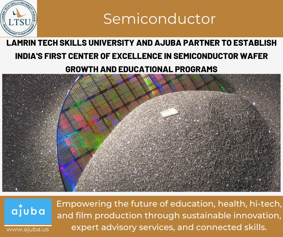
The establishment of the Center of Excellence (CoE) for Wafer Manufacturing by Lamrin Tech Skills University (LTSU) and Ajuba promises numerous benefits for India and the global semiconductor industry. Here are some of the key advantages:
- Technological Advancement: The CoE will drive technological advancements in semiconductor wafer manufacturing, leading to the development of more efficient and advanced semiconductor materials. This will enhance the competitiveness of the Indian semiconductor industry on a global scale.
- Research and Innovation: The collaborative research efforts within the CoE will foster innovation and breakthroughs in wafer growth techniques, crystal quality optimization, and defect reduction. This research will have far-reaching implications for the semiconductor industry worldwide.
- Skilled Workforce: The CoE’s educational programs, including specialized degrees in VLSI Design, Wafer Growth, Semiconductor Fabrication, and Semiconductor Testing & Packaging, will produce a highly skilled semiconductor workforce. This will address the skill gap in the industry and create a talent pool ready for the demands of the global semiconductor market.
- Global Education Hub: The School for Semiconductor & Nano Materials will attract students and researchers from around the world, making India a global hub for semiconductor education and research. This will promote cross-cultural collaboration and knowledge exchange.
- Industry Collaboration: The CoE will serve as a collaborative platform, bringing together industry leaders, researchers, and educational institutions. This collaboration will accelerate the development and adoption of cutting-edge semiconductor technologies globally.
- Economic Growth: The growth of the semiconductor industry through the CoE will contribute significantly to India’s economic development. It will create job opportunities, stimulate investments, and boost the manufacturing sector.
- Sustainability: The CoE will support research in sustainable semiconductor materials and processes, aligning with global efforts to reduce the environmental impact of technology manufacturing.
- Energy Efficiency: The adoption of advanced semiconductor materials like GaN and SiC will lead to greater energy efficiency in various applications, including electric vehicles and renewable energy systems. This aligns with global sustainability goals.
- Innovation Recognition: The CoE’s annual innovation awards will recognize outstanding contributions and encourage a culture of innovation among students, researchers, and professionals in India and beyond.
- Global Semiconductor Impact: The CoE’s focus on wafer growth in semiconductor materials like Silicon, GaN, and SiC will have a lasting impact on the global semiconductor industry, promoting the adoption of these materials in various applications.
In summary, the establishment of the CoE for Wafer Manufacturing by LTSU and Ajuba represents a significant leap forward in the semiconductor manufacturing sector. It not only benefits India but also has far-reaching implications for the global semiconductor industry, research, and education. This collaborative effort will shape the future of semiconductor technology, making it more competitive, sustainable, and innovative on a global scale. The Center of Excellence for Wafer Manufacturing recognizes the vast potential of GaN and SiC materials and aims to drive their adoption across industries, thereby contributing to the advancement of technology and the sustainability of energy systems.
The Center of Excellence for Wafer Manufacturing in Silicon, Gallium Nitride (GaN), and Silicon Carbide (SiC) is a pioneering initiative aimed at advancing semiconductor technology for a wide range of applications. With a keen focus on these materials, the center seeks to harness the unique properties of each to revolutionize the semiconductor industry.
Understanding GaN and SiC in Power Semiconductors
GaN and SiC are two distinct power semiconductor materials, each excelling in specific power and voltage requirements. Here’s a brief overview of their strengths:
Gallium Nitride (GaN):
- Best suited for devices with low to medium power and voltage requirements.
- Provides advantages like faster charging, faster switching, higher power density, and greater energy savings when compared to silicon chips.
- GaN chips find applications in mobile devices, chargers, home appliances, and consumer electronics.
- The GaN chips best fitted for applications under 1,000 volts and 10,000 watts.
Silicon Carbide (SiC):
- Better suited for medium to high power and voltage applications.
- Offers exceptional performance in electric vehicles, commercial solar and wind power, and industrial machine applications.
- SiC chips are known for their ability to handle higher voltages and power levels effectively.
We invite industry stakeholders, researchers, and educational institutions to join us on this transformative journey, where we aim to redefine the possibilities of semiconductor technology and make a lasting impact on multiple sectors.
Together, we will shape the future of semiconductor manufacturing, unleashing the full potential of Silicon, GaN, and SiC materials.
Contact Mr. Baljit Singh, CEO of Ajuba via email [email protected] for any further information.