Article 12
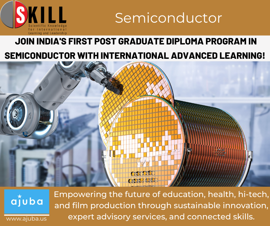
Welcome to Ajuba’s groundbreaking Post Graduate Diploma Program in Semiconductors with Advanced Learning Options! We are excited to embark on this transformative journey with you, equipping you with the necessary skills and knowledge to excel in the ever-evolving semiconductor industry.
Program Overview:
Our one-year Post Graduate Diploma program, complemented by a six-month internship, is meticulously designed to prepare you for a successful career in the field of semiconductors. Our curriculum covers a diverse range of topics, including Introduction to Nanoelectronics, IC Technology, Digital Electronics, Semiconductor Devices, Thin Films, Lithography Materials and Processes, Microelectronics Manufacturing, Microelectronics Research Method, and more. Expert instructors will provide hands-on training and guide you through real-world projects, ensuring you gain practical expertise in this dynamic domain.
Eligibility:
We welcome applications from candidates with any Engineering or Science Degree from a University or College. Whether you hold a 3-year or 4-year Engineering degree in Computer Science, Computer Engineering, Electronics, Electrical Engineering, Physics, Materials, or any other Engineering field, you are eligible to apply. Proficiency in English and selection through an interview process will be integral parts of the selection procedure.
Program Structure:
Here’s an overview of how the program is structured:
Building the Foundation:
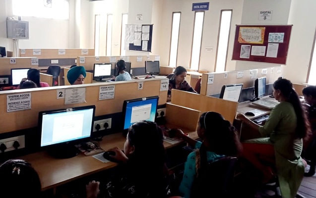
The initial nine months of the program will be dedicated to building a strong foundation in semiconductors and honing essential soft skills. At Rayat-Bahra University campus in Punjab, you will undergo comprehensive training in various technical aspects of semiconductors, including Introduction to Nanoelectronics, IC Technology, Digital Electronics, Semiconductor Devices, Thin Films, Lithography Materials and Processes, Microelectronics Manufacturing, Microelectronics Research Method, and more. Additionally, specialized training will focus on communication, teamwork, positive and professional attitude, stress management, and conflict resolution – soft skills vital for a successful career.
Advanced Learning:
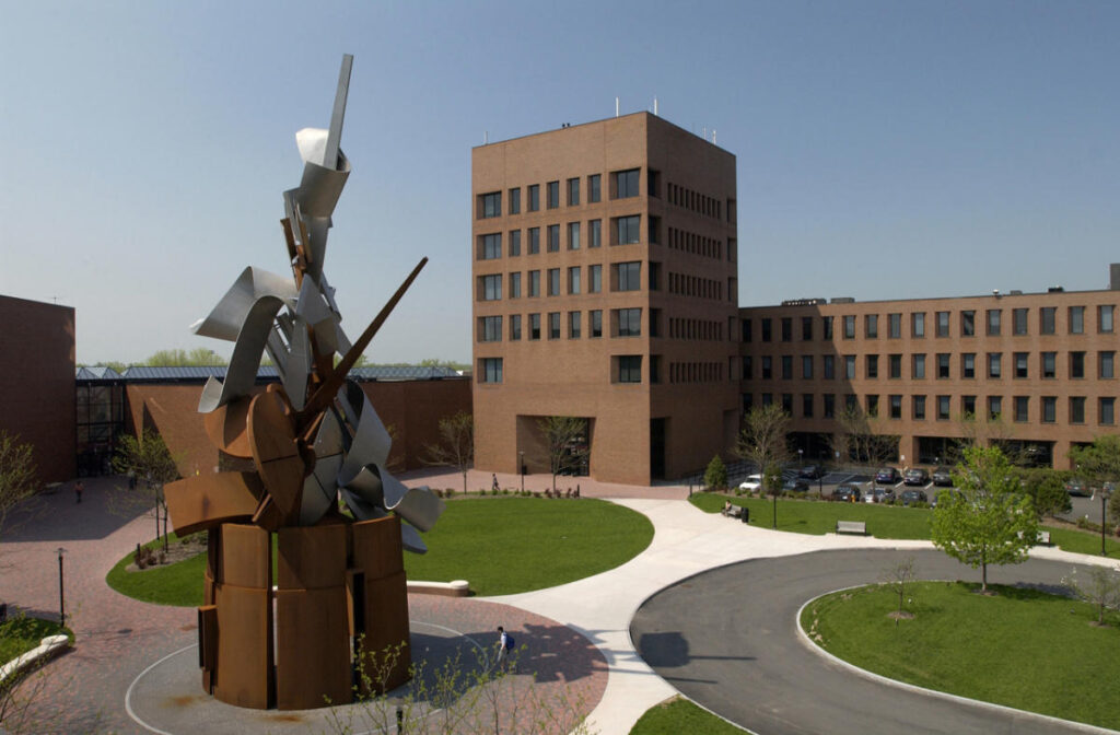
Following the foundation-building phase, you will have the privilege of choosing from three paths for advanced learning. You can opt for a ten-week advanced semiconductors learning experience at the prestigious Rochester Institute of Technology (RIT) in the United States. RIT’s expertise and innovation in semiconductors education will provide you with an international perspective on industry practices and challenges, widening your understanding of global trends.


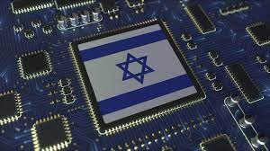
Alternatively, you can opt for advanced learning in Israel, a global hub for semiconductor innovation and research. This option exposes you to cutting-edge technologies, industry experts, real-world case studies, and solutions developed to tackle cyber threats. Your learning experience in Israel will be invaluable in staying ahead in the semiconductor industry.
For those who prefer to stay in India for advanced learning, we offer a unique opportunity to explore specific semiconductor design projects at Rayat-Bahra Campus. Alongside, you will have a one-week trip to Bangalore, gaining insights from design houses for your projects.


Internship Program:
Upon completing the one-year program, you have the option to participate in a six-month internship. We are committed to helping you secure internships, arranging a minimum of three interviews with potential companies. This internship provides the perfect platform to apply your knowledge and skills in real-world scenarios, gain hands-on experience, and further your professional growth. The compensation and job roles during the internship will be negotiated between you and the company.
Conclusion:
Ajuba’s Post Graduate Diploma program with advanced learning opportunities in the USA at RIT and in Israel is your passport to becoming a competent semiconductor professional. With access to state-of-the-art facilities, expert instructors, and real-world projects, you are primed to conquer the challenges and embrace the possibilities of the semiconductor landscape.
Embark on this extraordinary journey, and together, let’s make a lasting impact in the dynamic world of semiconductors.