Article 13 | August 4, 2023
As the semiconductor manufacturing field continues to progress, ion implantation remains an indispensable technology, ensuring the development of cutting-edge electronic devices. From its historical roots in the 19th century to the present, ion implantation has undergone significant refinements and advancements. Pioneers like Robert Van de Graaff and William Shockley laid the groundwork for its application in the semiconductor industry.
Robert Van de Graaff’s work in accelerator construction and the establishment of High Voltage Engineering Corp. (HVEC) were instrumental in shaping ion implantation technology. HVEC acted as an incubator for the essential equipment and expertise needed to build the first commercial ion implanters.
William Shockley’s visionary insight into ion implantation for semiconductor doping, demonstrated in his 1954 patent application, laid the foundation for the technology’s future applications. However, the expiration of his patent in 1974 coincided with the rise of the commercial ion implantation market, resulting in limited royalties for his pioneering ideas.
Over the years, researchers and experimenters honed the ion stopping hypothesis, allowing precise placement of ions based on energy and angle of implantation. Additionally, high-temperature post-implant annealing techniques were optimized, leading to improved crystal damage repair in semiconductor materials.
Join the FREE WEBINAR on ION IMPLANTATION
The advantages of ion implantation, such as precision, reliability, and repeatability, gradually displaced thermal diffusion as the dominant method of semiconductor doping. Companies like IBM and Western Electric designed and built early ion implanters for in-house use, while start-up companies began tapping into the technology, leading to the emergence of the commercial ion implantation market.
As semiconductor devices have become more complex, the number of implants needed for each integrated circuit (IC) has increased. While early semiconductor devices required only 6 to 8 implants, modern complementary metal-oxide-semiconductor (CMOS) ICs with embedded memory may contain more than 35 implants.
Energy and dose requirements in ion implantation applications vary significantly, spanning several orders of magnitude. To address this variability, semiconductor manufacturing plants utilize four types of ion implantation equipment: high-current, medium-current, high-energy, and ultra-high dose doping implanters.

As the name suggests, high-current implanters produce the highest beam currents, up to 25 mA. For high-dose applications, the greater the beam current, the faster the implantation, which means the output of more wafers per hour. Implanter makers have invested a great deal of effort in maximizing beam current, especially at the lowest energies. Although high-current implanters can produce beams in the 10-µA range, source instabilities make these beams unsuitable for low-dose applications. The short beam line of these implanters allows an energy range from <1 keV up to 100 to 200 KeV.
Medium-current implanters are designed for maximum dose uniformity and repeatability. Their beam currents are in the range of 1 µA to 5 mA, at energies of 5 to ~600 keV. The wafer-processing end stations can implant ions at angles up to 60° from the perpendicular to the wafer surface. This is essential for certain applications, such as anti-punchthrough implants, for example, in which dopants must be implanted partially underneath a previously formed gate structure. The lower operational cost of medium-current implanters when used for lower-dose applications and their ability to do high-tilt implants distinguish them from high-current implanters.
Last, only high-energy implanters can generate megaelectron volt ion beams. Commercial high-energy implanters produce beam currents for singly-charged ions up to ~1 mA. Energies for multiply-charged ions can be up to ~4,000 keV, with beam currents of ~50 µA. High-energy implanters can produce beams down to 10 keV, making them suitable for many medium-current applications as well. This additional functionality justifies the capital cost of these machines. High-energy implanters using both RF linear acceleration and dc acceleration are used widely today in semiconductor manufacturing.
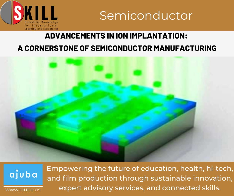
Semiconductor processors today use ion implantation for almost all doping in silicon ICs. The most commonly implanted species are arsenic, phosphorus, boron, boron difluoride, indium, antimony, germanium, silicon, nitrogen, hydrogen, and helium.
In conclusion, ion implantation has been a driving force in the semiconductor industry’s progress, enabling the creation of sophisticated and high-performance electronic devices. The contributions of pioneers, ongoing research, and the continued development of ion implantation equipment and techniques will ensure its continued significance in meeting the challenges of future semiconductor technologies. As the semiconductor industry continues to evolve, ion implantation will undoubtedly remain a cornerstone, guiding the way to the next generation of electronics and technology.
About BALJIT SINGH

Baljit Singh is an accomplished Founder & CEO with a proven track record in building successful businesses in manufacturing and services companies. With expertise in leadership and general management, Baljit has developed and implemented business strategies, led sales and marketing functions, and built motivated teams in turn-around environments. . Author of the Book, “My Experiments with Innovation,” he is a motivational speaker and gives talks on how to cultivate habits and change lifestyle to drive innovation. Baljit is currently driving cross border partnership between India-Israel-North America.