Article 15 | August 9th, 2023
Introductions
In the ever-evolving landscape of semiconductor manufacturing, ion implantation stands as a cornerstone process, critical to creating cutting-edge integrated circuits. As chip complexity continues to surge, so does the number of implantation steps. Modern CMOS integrated circuits with embedded memory can now require over 60 implantations to achieve the desired performance.
The semiconductor manufacturing realm relies on four distinct categories of ion implantation equipment: high-current, medium-current, high-energy, and ultra-high dose doping implanters. In article 13 we introduced the Ion Implantation concepts. Article 14 we introduced High Current Implanters. Here, we delve into the realm of Medium Current Implanters, shedding light on their significance and applications in semiconductor fabrication.
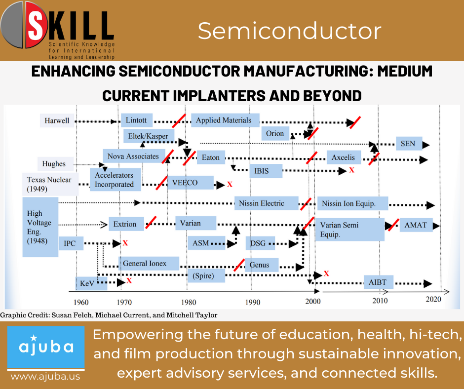
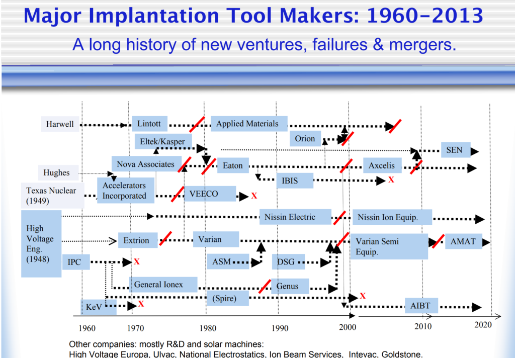
Tool Makers Journey
Susan Felch, Michael Current, and Mitchell Taylor illustrate well in their presentation on the long history major Ion Implantation new ventures, failures and merger.
Medium Current Implanters
Medium-current implanters have been meticulously designed to ensure maximum dose uniformity and repeatability. These workhorses of the fabrication process maintain beam currents ranging from 1 µA to 5 mA, operating at energies of 5 to around 900 keV (triple-charge), with dose levels spanning from E11 to E14. An essential attribute of medium-current implanters lies in their ability to implant ions at angles of up to 60° relative to the wafer surface’s perpendicular orientation. This angular flexibility becomes crucial for specialized applications such as anti-punch through implants, where precise implantation underneath pre-existing gate structures is necessary. The utilization of medium-current implanters for lower-dose applications, coupled with their aptitude for high-tilt implants, sets them apart from their high-current counterparts [1].
In the context of CMOS transistor fabrication, scaling brings both advancements and challenges. One pressing challenge is the escalating leakage current due to scaling. The creation of highly activated ultra shallow junctions (USJ) that retain stability and abruptness poses a significant hurdle. To surmount this challenge, the industry has turned to innovative damage engineering strategies, including cryogenic implant technology and co-implants. Medium current implanters have found their place, serving shallow wells and playing crucial roles in tasks such as threshold voltage adjustment and channel engineering [2].
The concept of cryogenic ion implantation has gained prominence. Traditionally, Boron source/drain doping for PMOS transistors was carried out using high current ion implanters. However, this practice led to elevated wafer temperatures that could deform photoresist masks. Cryogenic cooling, even extending to medium current applications like HALO, emerges as a solution to maintaining precise wafer temperatures even as low as -100°C.
In the realm of molecular dopants, the industry has seen the evolution from BF2 to the use of carborane (C2B10H12 – “CBH”) for PMOS source/drain doping. CBH introduces carbon into the lattice during doping, offering benefits such as reduced end-of-range (EOR) defects, enhanced dopant activation, and minimized lateral diffusion. Cryogenic implantation has shown particular promise in the activation and reactivation of boron in annealed silicon, bolstering its utility [3].
Precision is a core concern in ion implantation, and the introduction of tighter angle control becomes essential. As technology advances, post-implant anneals have become less effective in smearing out dopant profile variations caused by angle discrepancies. Achieving uniformity, both on the micro and macro scales, is pivotal. This uniformity is governed by ion beam dynamics and wafer handling capabilities. Developments like ribbon beams have revolutionized beam transport, and innovative wafer handling systems utilizing flexible rotational platforms are expanding the field’s capabilities.
Ultimately, as the industry marches towards enhanced device performance, medium current implanters emerge as versatile tools, enabling critical processes such as threshold voltage adjustment and shallow well implants. With the integration of groundbreaking concepts like cryogenic cooling and innovative molecular dopants, these medium current implanters continue to play a pivotal role in the semiconductor landscape.
References
- James L. Kawski, Leveraging ion implant process characteristics to facilitate 22nm devices, Solid State Technology | Volume 54 | Issue 3 | March 2011
- F. Khaja, B. Colombeau, T. Thanigaivelan, D. Ramappa, T. Henry, “Benefits of Damage Engineering for PMOS Junction Stability,” 2010 Inter. Conf. on Ion Implant Technology, Kyoto, Japan, to be published.
- C.I. Li, P. Kuo, H.H. Lai, K. Ma, R. Liu, H.H. Wu, et al., “Enabling Solutions for 28nm CMOS Advanced Junction Formation,” 2010 Inter. Conf. on Ion Implant Technology, Kyoto, Japan, to be published.

Baljit Singh is an accomplished Founder & CEO with a proven track record in building successful businesses in manufacturing and services companies. With expertise in leadership and general management, Baljit has developed and implemented business strategies, led sales and marketing functions, and built motivated teams in turn-around environments. Author of the Book, “My Experiments with Innovation,” he is a motivational speaker and gives talks on how to cultivate habits and change lifestyle to drive innovation. Baljit is currently driving cross border partnership between India-Israel-North America.
Website: www.ajuba.us
Email: bsingh@ajuba.us