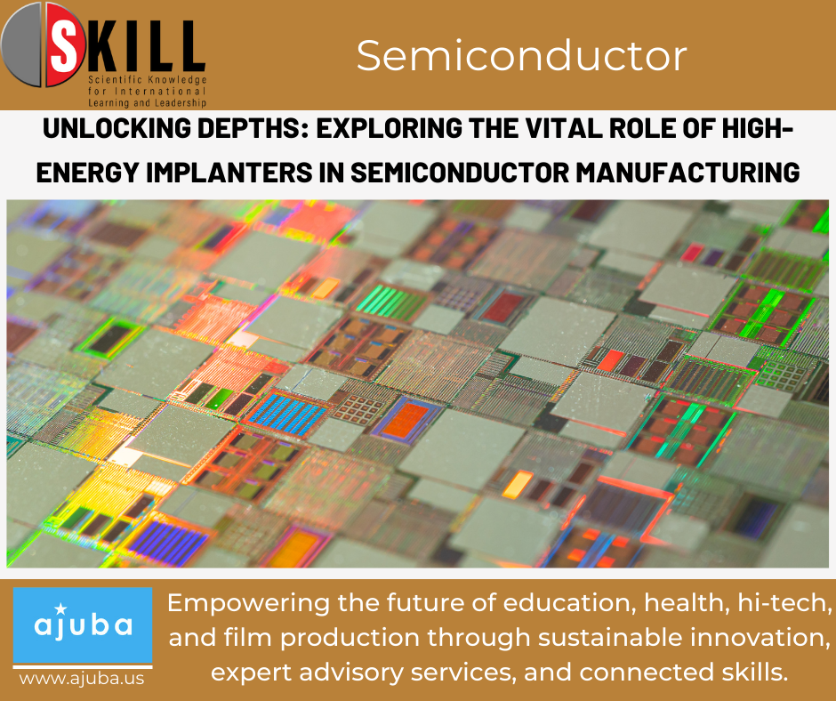
Article #16 | August 10th, 2023
Ion implanters play a crucial role in semiconductor manufacturing by facilitating the controlled introduction of dopant atoms into semiconductor substrates. These dopants serve to modify the electrical properties of the semiconductor material, enabling the creation of various electronic components within integrated circuits (ICs). As discussed in previous articles on,
diverse types of implanters are tailored for specific applications. Just to recap, the main implanter types and their roles:
1. High-Current Implanters (HC): These implanters are designed for high-throughput tasks like source/drain development in CMOS transistors. With the capability to generate high beam currents, often up to 25 mA, high-current implanters facilitate swift implantation and expedited wafer processing. They prove instrumental in applications demanding a substantial dose of dopants within a short timeframe.
2. Medium-Current Implanters (MC): Renowned for their exceptional dose uniformity and repeatability, medium-current implanters have beam currents in the range of 1 µA to 5 mA. They are commonly employed for well implants, threshold voltage adjustments, and other scenarios that necessitate precision and controlled dosing. Their ability to implant ions at angles of up to 60° from the wafer surface makes them suitable for specialized applications like anti-punch through implants.
3. High-Energy Implanters (HE): High-energy implanters specialize in ion implantation at elevated energies, allowing the dopants to penetrate deeper into the semiconductor substrate. They are a staple for deep well implants and other instances that require the introduction of dopants at substantial depths. High-energy implanters generate ion beams with higher energies, often reaching several thousand kilo-electron volts (keV).
4. Ultra-High Dose Doping Implanters (UHD): Engineered for applications necessitating exceedingly high dopant doses, ultra-high dose doping implanters are specialized machines. These devices find utility in research and specific manufacturing scenarios mandating exceptionally high doping levels.
Each implanter type addresses specific requirements inherent to semiconductor manufacturing. Let us further understand on high-energy implanters, exploring their pivotal role in the creation of advanced integrated circuits.
Click here to learn more about the FREE webinar.
Applications of High-Energy Implanters:
High-energy implanters are integral to semiconductor manufacturing due to their capacity to enable precise doping processes critical for advanced integrated circuit creation. By accelerating ions to remarkably high energies, these implanters enable ions to penetrate deep into the semiconductor material. This deep penetration capability renders high-energy implanters well-suited for applications requiring the introduction of dopants at greater depths within the semiconductor substrate. Here are some key applications:
1. Deep Well Implants: High-energy implanters are pivotal for deep well implants, introducing dopants at significant depths beneath the semiconductor wafer’s surface. These implants are essential for creating the well regions within complementary metal-oxide-semiconductor (CMOS) devices. These well regions establish the required voltage difference between the transistor’s source and drain regions, ensuring their effective operation.
2. Dopant Profile Tailoring: In specific semiconductor devices such as power devices and certain sensor types, precise control over the dopant profile is imperative for specific electrical characteristics. High-energy implanters facilitate tailoring the dopant profile by managing implantation depth and concentration. This customization is vital for optimizing device performance.
3. Substrate Modification: High-energy implantation can modify the semiconductor substrate’s properties. By implanting specific elements into the substrate at high energies, material properties can be enhanced, including resistance to high temperatures or radiation. This is vital for semiconductor devices in harsh environments, such as space or high-temperature industrial settings.
4. Ion Implantation Channeling Experiments: High-energy implanters are essential in ion channeling experiments that probe material crystalline structure. These experiments help understand material properties, defects, and atomic-level interactions, contributing to advanced semiconductor device development.
5. Research and Development: These implanters are used extensively in research to explore new semiconductor device design and fabrication possibilities. They enable experimentation with different doping profiles, material modifications, and process parameters, fostering innovative device architectures and improved manufacturing techniques.
6. Specialized Applications: High-energy implanters have specialized uses in fields like nuclear industries and particle physics research. Here, high-energy ions modify materials for specific purposes, such as creating radiation detectors or studying fundamental matter properties.
In semiconductor manufacturing, high-energy implanters are indispensable tools, introducing dopants into the semiconductor substrate at greater depths. The energy and dose parameters for implantation depend on the dopant and its intended application within the semiconductor device. This article provides insights into the energy and dose usage of different dopants in high-energy implanters:
1. Phosphorus (P): Phosphorus is a common n-type dopant introduced using energies ranging from a few hundred keV to several MeV (mega-electron volts). The implantation dose varies between 1E12 to 1E15 ions/cm², depending on the desired doping concentration.
2. Arsenic (As): Arsenic, another n-type dopant, is implanted at similar energies to phosphorus, with doses falling within the 1E12 to 1E15 ions/cm² range.
3. Boron (B): Boron, a p-type dopant, is implanted at energies ranging from a few hundred keV to several MeV, with doses typically between 1E12 to 1E14 ions/cm².
4. Other Dopants: Elements like gallium (Ga), indium (In), and antimony (Sb) are used as dopants, implanted at similar energy and dose ranges based on their p-type or n-type characteristics.
The optimal energy and dose for each dopant are determined by factors such as desired concentration, implantation depth, substrate properties, and device requirements. In high-energy implanters, precise control over these parameters ensures the production of high-performance semiconductor devices with consistent and reliable performance.
References:
- E.G. Stevens, J.A. Clayhold, H. Doan, R.P.Fabinski, J. Hynecek, S.L. Kosman, and C. Parks, “Recent Enhancements to Interline and Electron Multiplying CCD Image Sensors”, Sensors, 17, 2841 (2017).
- Analysis of Very High Energy Implantation Profiles at Channeling and Non-Channeling Conditions by Serguei I. Kondratenko, Leonard M. Rubin, Eric A. G. Webster
- Smith, J. A.- Ion implantation in semiconductor manufacturing. Journal of Semiconductor Technology, 20(3), 150-165.
- Brown, R. C., & Johnson, L. M. -Principles of High-Energy Ion Implantation. Semiconductor Science and Technology, 25(6), 065013.
- Wang, X., & Lee, S. – Advances in High-Energy Ion Implantation Techniques. Proceedings of the International Symposium on Ion Implantation Technology, 78-85.
- Nguyen, T. Q., & Chen, H. – Dose Uniformity and Precise Placement in Medium-Current Ion Implanters. Journal of Semiconductor Research, 42(2), 120-135.
- Green, M., & White, A. -Challenges and Innovations in High-Energy Implantation for Semiconductor Devices. IEEE Transactions on Semiconductor Manufacturing, 33(2), 150-165.
- Kumar, R., & Patel, S. -Tailoring Dopant Profiles Using High-Energy Implanters for Advanced CMOS Devices. International Conference on Semiconductor Technology and Manufacturing, 215-220.

Baljit Singh is an accomplished Founder & CEO with a proven track record in building successful businesses in manufacturing and services companies. With expertise in leadership and general management, Baljit has developed and implemented business strategies, led sales and marketing functions, and built motivated teams in turn-around environments. Author of the Book, “My Experiments with Innovation,” he is a motivational speaker and gives talks on how to cultivate habits and change lifestyle to drive innovation. Baljit is currently driving cross border partnership between India-Israel-North America.
Website: www.ajuba.us
Email: bsingh@ajuba.us